The long-awaited 2017.12-rc1 release is now available on GitHub! This release includes a stable version of Automatic Gain Control (AGC) for the bladeRF, as well as a new way of using a configuration file to quickly configure your bladeRF with your favorite settings. The software features are available for all bladeRF devices.
This remainder of this blog post dives into the internals of the bladeRF’s AGC.
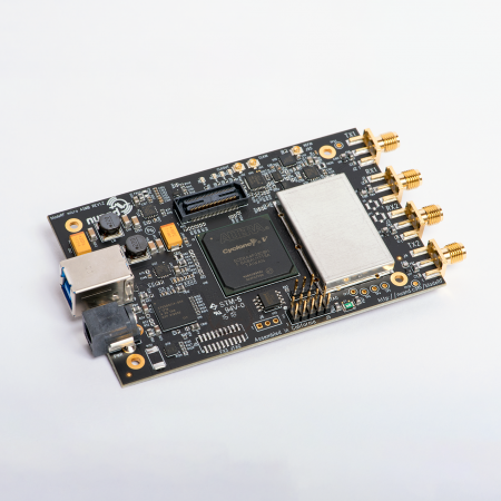
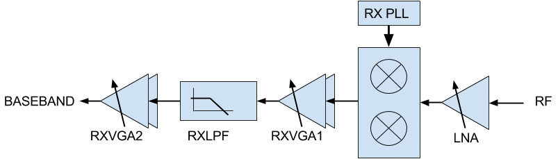
The bladeRF’s RF front-end (pictured below) is composed of several RF switches, baluns, and the LMS6002D RF transceiver IC. The internal RX path of the LMS6002D has three gain stages: the low-noise amplifier (RXLNA), and two variable gain amplifiers (RXVGA1 and RXVGA2).
Amplification at the front-end will increase the peak-to-peak voltage of a signal picked up by an antenna to a level that allows for an analog-to-digital converter (ADC) to digitize it. Even a moderately strong RF signal that is received at -65 dBm is only 356 microvolts peak-to-peak (µVpp) when incident on a 50 Ω antenna. This voltage swing is far too low to be digitized by inexpensive ADCs used in consumer RF applications. Therefore, the signal must be amplified by several tens of dB to bring it up to a usable voltage swing. There is no industry standard, but in general, the internal ADCs used in RF applications need the analog baseband signal to enter the ADC at more than 280 mVpp.
As with most LNAs, the RXLNA of the LMS6002D offers a very modest gain (6 dB), but its primary design goal is to offer a low noise figure (NF), meaning it adds very little noise to the initial signal. The VGA stages following the LNA offer much higher gains (up to 30 dB!), but at the expense of higher noise figures. The gains are multiplicative, so the total system gain may be calculated by summing the dB gains of each of the 3 stages. On the other hand, calculating the total system noise figure requires a more complicated equation, known as Friis’ formula:

In Friis’ formula, Fn and Gn is the noise figure and gain at each stage n. By inspecting the equation, it quickly becomes apparent that the system’s total noise figure is most greatly impacted by the noise figure of the first element (F1), and somewhat less and less at each additional stage. This is why it is very important to choose an amplifier with a very low noise figure (specifically, an LNA) for the first stage, even if it only offers a modest signal gain. It follows from this equation, that to minimize the impact of noise on a signal received by the bladeRF, we must increase RXLNA first, followed by RXVGA1, and lastly RXVGA2 until the target gain is achieved.
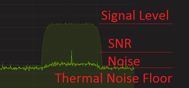
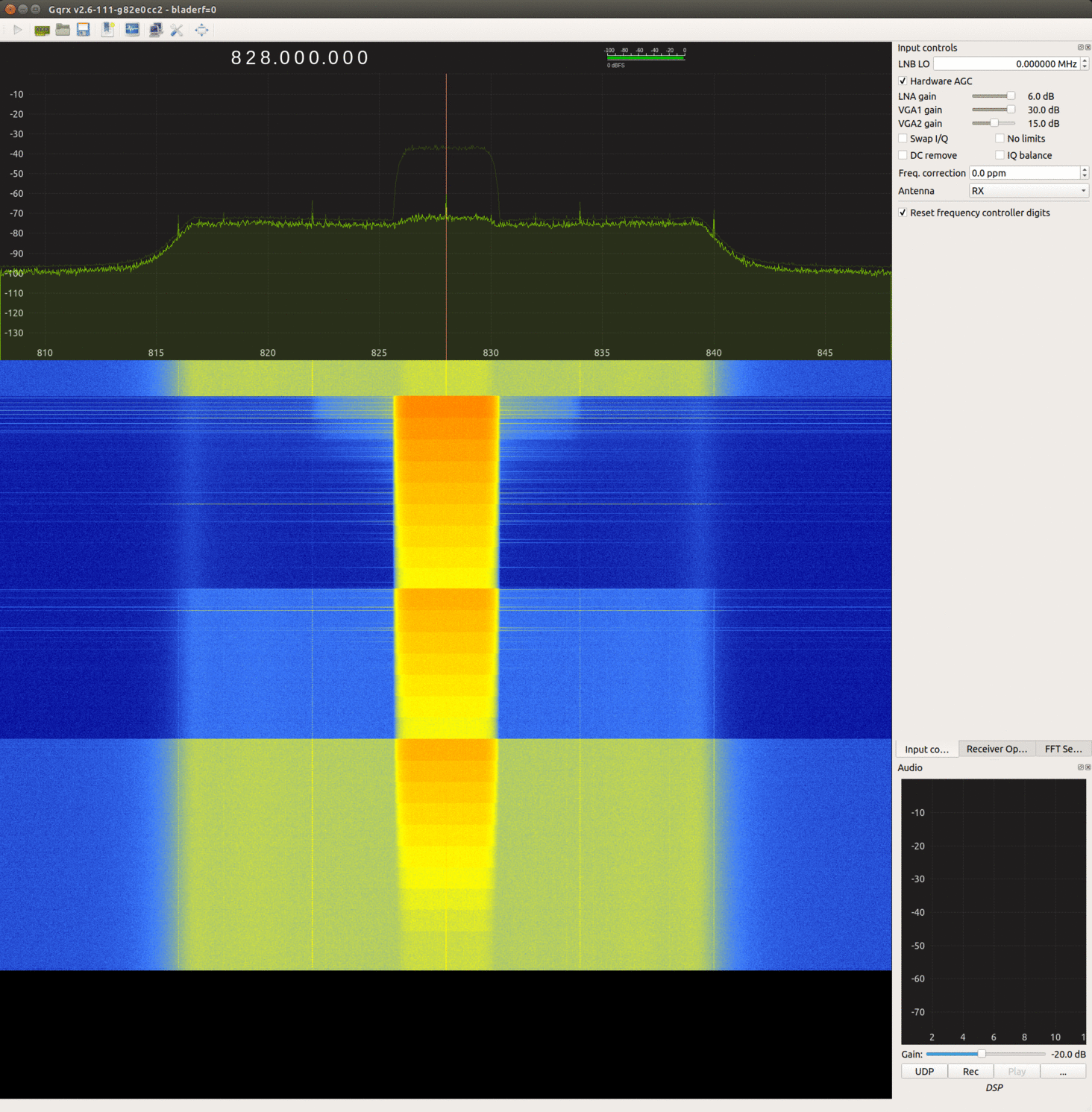
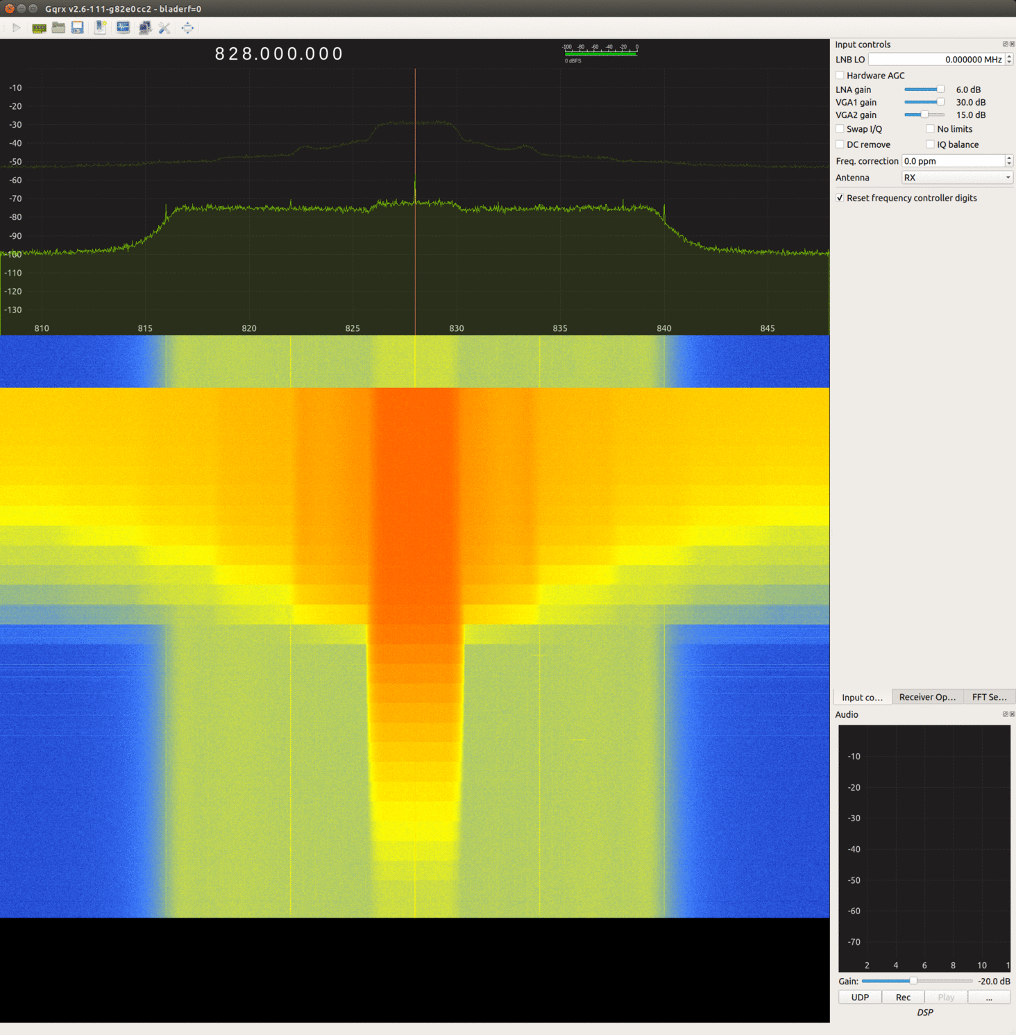
This process can be visualized by looking at an incoming tone in a spectrum analyzer application such as gqrx. In the previous image, the central spike is the DC offset, and not an actual signal.The signal-to-noise ratio (SNR) can be thought of as the deflection of an incoming signal above the noise floor. This distance is commonly expressed in dB. Looking at an incoming tone in gqrx, the distance can be measured as the difference between the peak of the incoming signal and the noise floor. Amplifiers indiscriminately amplify both noise and signal, so amplifiers must be chosen in a way that maintains that relative distance (SNR) between the noise floor and the peak of a signal, while also amplifying very weak RF signals until they can be digitized by a reasonable ADC. The higher a component’s noise figure, the more it destroys the SNR by decreasing that distance.
The bladeRF’s RF front-end has a quadrature 12‑bit ADC, with an Effective Number of Bits (ENOB) of about 10 bits. At roughly 6 dB of static range per bit, the bladeRF has a static range of 60 dB. If, for example, the RX gains are adjusted in such a way that the bladeRF can receive a signal at +10 dBm without clipping, the least powerful signal it could possibly receive is ‑50 dBm. Alternatively, if the RX gains are configured in such a way that the bladeRF is barely sensitive enough to detect a ‑100 dBm signal, any signal that is stronger than ‑40 dBm will be clipped, as the digitized value would fall outside the signed, 12‑bit range of the ADC (±2047).
Usable RF signals “in the wild” generally have power levels between -120 dBm and +10 dBm at the receiver. This is a 130 dB range, yet the hardware can only cleanly receive 60 dB at a time! Receiving signals across that entire range, without missing weak signals or clipping strong ones, requires dynamically adjusting RX gains using an Automatic Gain Controller (AGC). These systems work by waiting in the highest gain setting, and quickly decreasing the system gain when a stronger signal is received. When the strong signal weakens or disappears, the AGC returns to a higher gain level, ensuring the system won’t miss weak signals.
The bladeRF’s AGC is consists of a power measurement block, a master controller, and a gain driver for the LMS6002D.
The power measurement block is a simple 2‑tap IIR of the incoming signal power (
The controller uses that filtered power level to decide whether to command a gain change. If the incoming power falls below a certain threshold, the controller commands a gain increase. Conversely, when the signal’s level rises above another threshold, the gain is decreased. These hand-picked thresholds are chosen to provide hysteresis for stability, as well as ample headroom for transient power increases. Since these values are very device‑specific, they must be empirically derived and tested for each new kind of RF front-end.
The gain driver has three states: the high-gain state (also known as the idle state), the mid-gain state, and the low-gain state. The code snippet in bladerf_agc_lms_drv.vhd, specifies the estimated signal level range for each gain state, along with the corresponding RXLNA, RXVGA1, and RXVGA2 settings. The states are tabulated below:
Gain state
Incoming Signal Power Range
RXLNA
RXVGA1
RXVGA2
HIGH_GAIN
-82 dBm to -52 dBm
6 dB (Max)
30 dB
15 dB
MID_GAIN
-52 dBm to -30 dBm
3 dB (Mid)
30 dB
0 dB
LOW_GAIN
-30 dBm to -17 dBm
3 dB (Mid)
12 dB
0 dB
Since the bladeRF’s AGC bases its decisions on the filtered history of the instantaneous power of samples (
To use the AGC, first ensure you have a new DC calibration table that includes AGC data. After upgrading libbladeRF and bladeRF-cli, a new DC calibration table should be generated following the Generating a DC offset table instructions on our Wiki. Also ensure that you’re using FPGA version 0.7.1 or later. Once the new DC calibration table is in place, run bladeRF-cli -i and enable the AGC by running set agc on.
Also new in 2017.12‑rc1: libbladeRF support for local and global configuration file! If the tool you are using doesn’t support setting certain bladeRF-specific options, they can now be set using a bladeRF.conf file. To enable the AGC this way, write the following line to a bladeRF.conf in your local or global bladeRF directory: agc on
The AGC can be see in action by capturing samples from a Vector Signal Generator using the bladeRF.
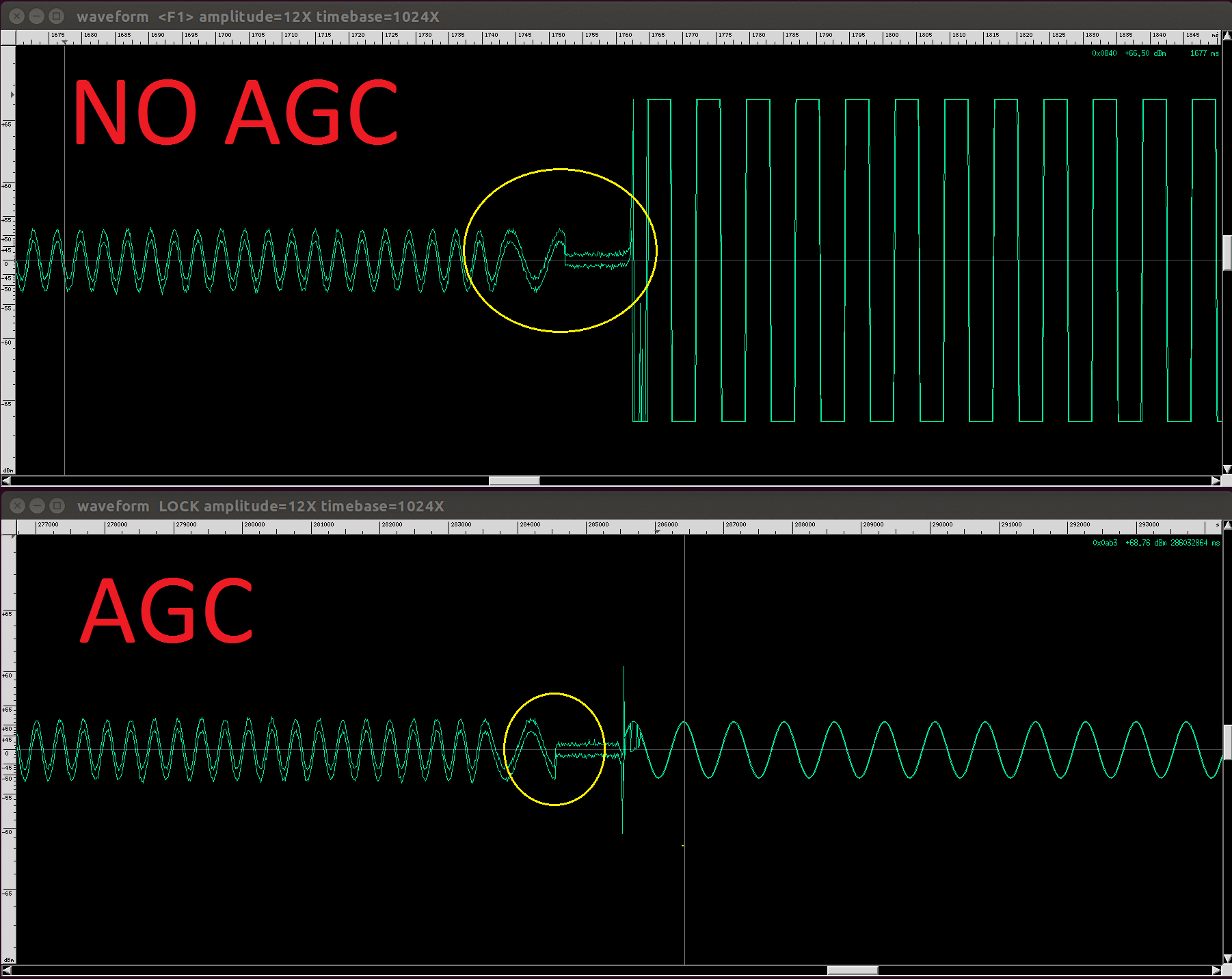
A VSG was configured to transmit a continuous wave signal at -70 dBm and -25 dBm with a 50% duty cycle over a 1ms period. The lower power signal was also configured to be at a slightly higher frequency. Baudline was used to zoom in on the rising edge of the signal coming from the VSG. The flatline (in the yellow circles) is an artifact caused by the VSG. Basically, the VSG disables its output when it adjusts its output power.
It is evident that when the bladeRF’s AGC is disabled, a strong incoming signal will cause the RF front-end to clip, and turn a sinusoidal wave into a square wave! The bottom capture shows the AGC very quickly latching on the new higher power signal (the short burst after the yellow circle).
Below is a longer capture of multiple rising and falling edges, with and without the AGC being enabled.
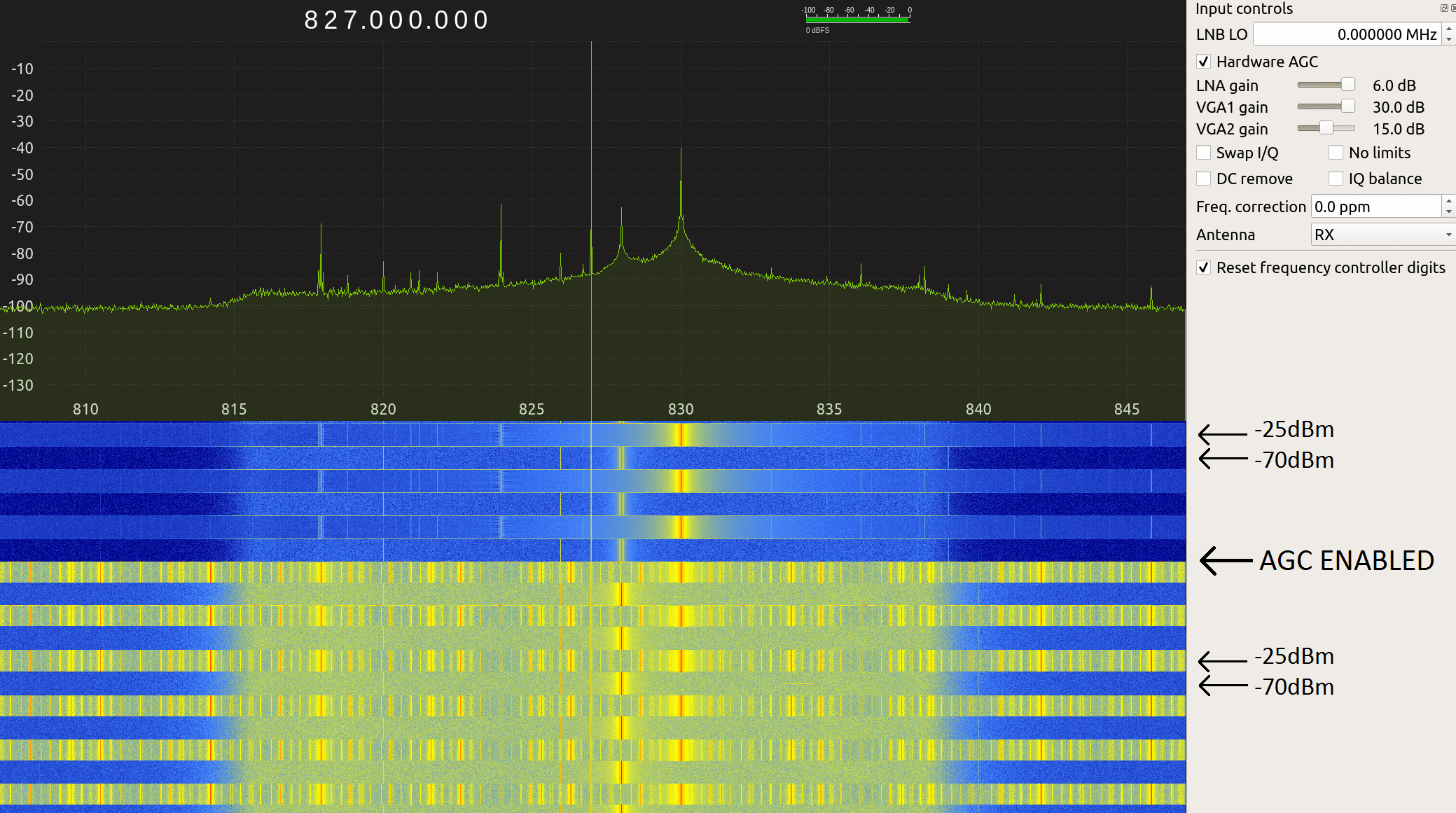
Lastly, the bladeRF was subjected to a power ramp from -100 dBm to -20 dBm at 3 dB steps. Without looking at the configuration panel, can you tell which capture was taken with the AGC enabled?