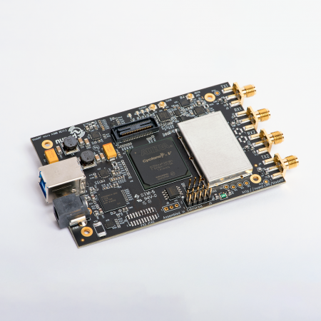
We got a call earlier this week letting us know the assembled boards were ready to be picked up!
The build quality looked amazing, and from a first inspection it seems as though most components were placed correctly. The orientation of the LEDs was harder to determine due to their smaller size but those checked out as well.
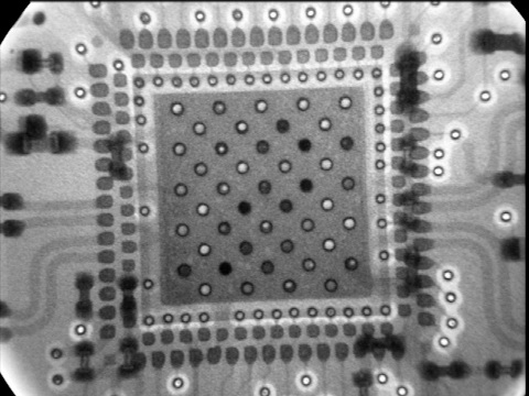
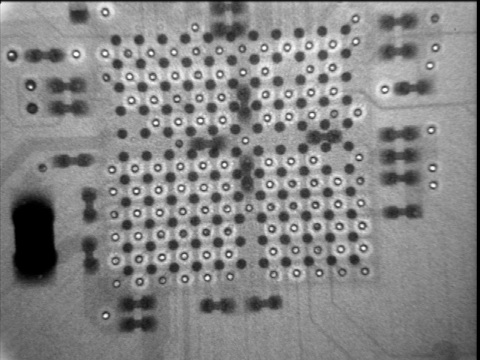
With high density interconnects, visual inspecting BGAs and fine pitch QFNs is not possible so we had X-ray the boards.
Some of the thermal relief VIAs wound up getting plugged, however it is evident that none of the solder leaked outside of the boundaries of the thermal relief pad. The darker spots that can be seen between the two rows of the DQFN are 0201 capacitors and resistors underneath the LMS part.
We were a little worried about the manufacturability of our boards when the PCB house told us we were getting close to pushing their capabilities, however the X-Ray shows pretty clearly that all of the VIAs underneath the FX3 are well defined and symmetric.
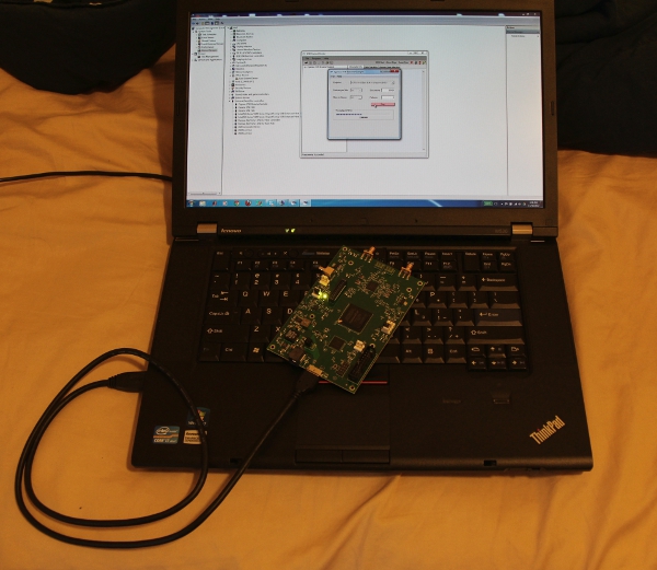
After making sure there were no shorts by checking resistance between the different power supplies and ground, it was time to power up the board. Luckily no sparks came flying out. After checking that all 7 key power domains were at the right voltage, the board was plugged in to a running laptop. The Cypress development tools quickly detected the Cypress USBBootloader that boots from ROM when the SPI flash does not contain a valid image. Within its first few minutes of operation, the Bulk Loopback benchmark utility was running and showing round-trip throughput of 250MB/s. Theoretically, the FX3 should be able to do nearly 400MB/s but Window’s XHCI driver has some catching up to do when compared to Linux 3.5.
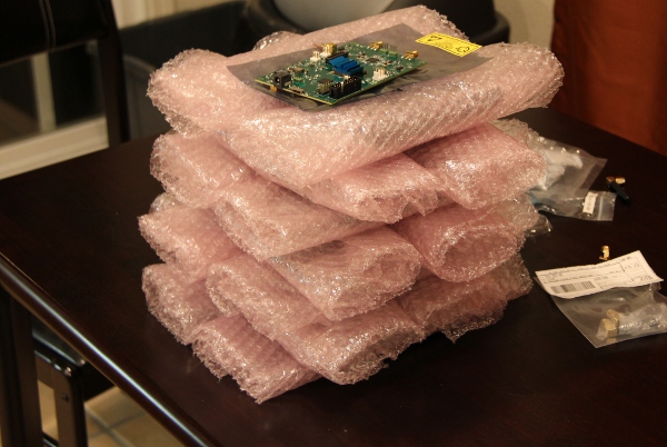
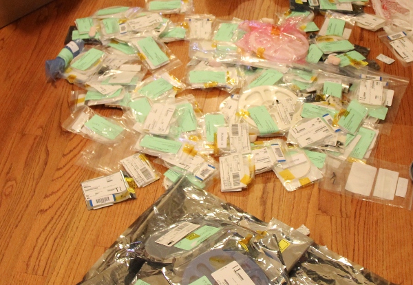
Lastly, builds of this run usually tend to leave a lot of left over components, here’s a few pics of the mess we’ve created:
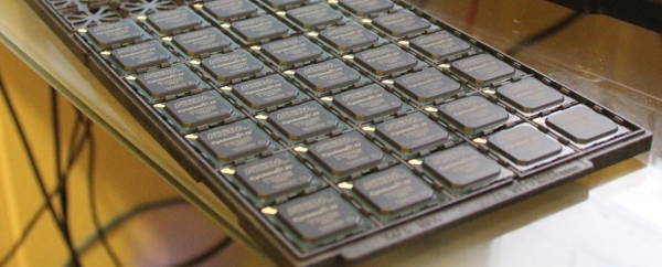
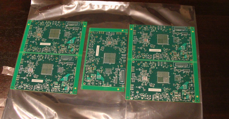
Left over cyclone 4s


Recent Comments