Posts by Robert Ghilduta

Read More

Yet another January update


We have spent the last couple of weeks further developing the platform and talking with part distributors. All of our parts at this point are in stock, and those that aren’t have reasonable lead times. We are taking these steps to ensure that if we do go to mass production there will be no hiccups.

As for some other exciting news, we recently got our hands on the first of several pieces of test equipment we will need to develop our intended examples and expansion boards. Having this sort of equipment at home is much more convenient than constantly scheduling lab time weeks in advance!

IMG_0094


As a sanity check, we ran a conducted RF chirp on the bladeRF at 500MHz to see its maximum bandwidth capabilities. In previous experiments, we have seen about 28MHz of occupied bandwidth, which this run seems to agree with.


28_obw


The spectrum analyzer was used to capture a spectrum of spurs over the bladeRF’s frequency range on the RX side. Besides the occasional spur, the noise floor of the device is surprisingly good.

rx_spurs


Here is the same sort of spectrum capture but on the TX side, and again the spectrum looks pretty clear with the exception of a few spurs which appear to be related to the main 38.4MHz clock. Spurs this low on the TX side really don’t matter since they are so far down below the TX output power of the LMS that they will no be able to significantly interfere with any transmissions or even influence


tx_spurs

Read More

2013 Update

Quick announcement, we have a few spots left in our beta tester program for researchers. Requests should be sent to [email protected] along with a short bio and description of your intended application.

Thank you all for the interest you have shown, we have successfully completed our tester program. Stay tuned for updates and a big announcement in late January.


We are quickly nearing a point with software support where we will be confident in doing a general release after doing a little clean up on the code. The soon to be released software support will be completely open source and will contain VHDL and FX3 source code, Linux drivers, user mode utilities, and a simple GNURadio block.


Additionally, we’ve been making great progress on the basic modulation scheme examples. One of the introductory tutorials explains the the development of a wireless UART bridge starting from scratch. Before complicating the examples with too much embedded and driver development, we are utilizing the onboard Cyclone 4 FPGA to modulate data using FSK and demodulate it on the receiving end.

The first screenshot shows signals internal to the FPGA captured using a soft-logic analyzer known as SignalTap. Data that is received by the FPGA on fx3_uart_txd is modulated and turned into I and Q samples that are rendered using the analog visualizer in SignalTap. The FSK modem is in loopback mode in this example, this allows us to measure the group delay by counting the number of clock cycles it takes a bit to come back around, in this case it’s roughly 45 clock cycles at 100MHz, or 450ns. The demodulation signals, specifically I and Q are shown in the bottom SignalTap capture.


fsk_uart

UART FSK modulation signals


fsk-chirp

UART FSK demodulation signals


Read More

Achieving 290MB/s over USB 3.0


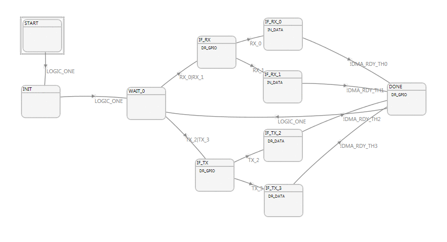
The FX3 contains a peripheral known as the GPIF, which is a 32bit 100MHz state machine based bus. This core has access to 4 DMA channels to the rest of the FX3 and executes independent of the on-chip ARM microcontroller. To use the GPIF to transfer data between the FX3 (subsequently the host PC) and the FPGA a state machine was designed using the GPIF Designer (available from Cypress). Since the bladeRF can operate at full-duplex a versatile state machine had to be designed, keeping in mind the limitations of the FX3. Fortunately, the FX3 offers DMA double buffering, which allows the GPIF to read data using one DMA channel while allowing another DMA channel to copy data from USB endpoints. Double buffering both RX and TX allows the bladeRF to fully saturate the GPIF bus, allowing for nearly 400MB/s data throughput.

Due to a limitation of the GPIF, the FPGA keeps a single bit of state that indicates which RX and TX DMA channels were used last. States IF_RX_0, and IF_RX_1 read data from the GPIF using DMA channels 0 and 1 respectively, and move it in internal DMA buffers, while states IF_TX_2 and IF_TX_3 write data to the GPIF. To operate at maximum efficiency in full-duplex mode the GPIF will likely have one TX and one RX buffer being sent over USB as another set of RX and TX buffers are being operated on by the GPIF. Due to the round-robin DMA channel selection requirement of the FX3, GPIF data read operations have to alternate between utilizing DMA channels 0 and 1 to push data to the FX3; the same applies to GPIF write operations, which in this application have to alternate between IF_TX_2 and IF_TX_3 (DMA channels 2, and 3). To further complicate issues, the delivery of USB packets is not guaranteed to be interlaced, so it unlikely that a USB BULK IN packet will follow a USB BULK OUT packet therefore the state machine has to be versatile to anticipate executing multiple GPIF data reads followed by multiple GPIF data writes.

Keeping all of this in mind, the solution we chose was to have the FPGA be notified of which DMA channels have data, and which are free. This way the FPGA can also control the state machine to tell it which DMA channels to use; the GPIF state machine does not have general purpose registers or enough specific purpose registers to keep track of scheduling all 4 DMA channels in such a way.


fx3-gpif-fsm


Once flashed to the FX3, the Cyclone 4 FPGA was instrumented using SignalTap and the GPIF bus was analyzed. Signals ctl[8] and ctl[11] are indicators that the GPIF is consuming data buffers from DMA channels 2 and 3, respectively. Signals ctl[10] and ctl[12] show the GPIF sitting idle. Signals ctl[6] and ctr[7] are DMA empty status flags belonging to DMA threads 2 and 3, respectively.


state_capture


The maximum throughput of the GPIF can be calculated by measuring the amount of time elapsed between sequential 1024-cycle 32-bit buffer transfers. By selecting the start of the first full buffer at time 1088 (1024+64), and subsequent data buffer as starting at roughly 2432, the elapsed time is calculated to be 13.44 microseconds. Transferring 1024 * 32bit in 13.44 microseconds corresponds to a throughput of 290MB/s.